With the development of technology, the size of monocrystalline silicon wafer is increasing.
Before 2012, the size of monocrystalline silicon wafers was mainly divided into two types: 156mm margin and 125mm margin.
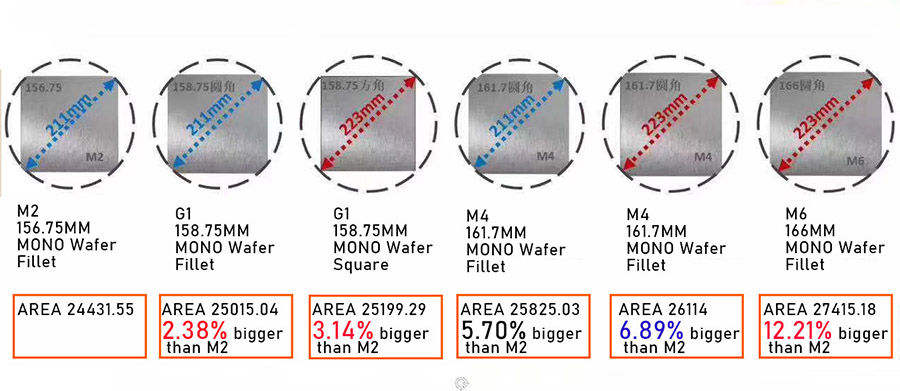
At the end of 2013, longi, Zhonghuan and other five major manufacturers took the lead in unifying the silicon wafer size with a standard of 156.75mm
At the beginning of 2020, Longi, Zhonghuan introduced large silicon wafers with the sizes of 166mm ,182mm and 210mm respectively. The reason is that the increasing size of silicon wafers can bring many aspects of cost reduction and efficiency increase for all downstream links. The large silicon wafer cost reduction mainly comes from the below two factors:
- Capacity is increased after wafer bigger ,the corresponding equipment ,labor cost do not need to increase . Solar cells production line production rate to be calculated by pieces.when wafer’s area is larger, the capacity increases, the corresponding expense as labor cost,equipment deprecition is decline. M12 than M2 solar cells can save USD013 /W, drop 25.6%.It also happened on production of solar modules.
- From the side of solar modules and power station, after the size of wafer and solar panelincreases, the consumption of frame ,PV ribbon,EVA etc increases correspondingly, but the increase is less than benefits come from bigger wafer.
Large wafers can also increase the efficiency of the solar modules.Due to the use of larger wafers and cells, the area occupied by the cells is increased, thus increasing the power of the solar modules while the efficiency of the cells is the same.It is estimated that under the same efficiency of cells,The efficiency of the solar module in M12(210mm) can be increased by 0.7% compared with M2(156.75mm).